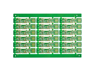


PCB for embedded devices
The characteristic of small mobile devices is that more and more passive components require higher density installation. Unfortunately, the surface mounting area of traditional surface mount technology (two-dimensional implementation) cannot support these components. That's why embedded PCB technology is used to achieve 3D implementation.
We independently developed a connection process using laser and electroplating, in addition to using solder materials during the welding process, and have records of large-scale production for these two processes.
Feature
Reduce surface mount area by embedding chip components (resistors/capacitors)
Improving electrical performance through shorter wiring distances between surface mounted integrated circuits and embedded components
Short spacing between components and better heat resistance
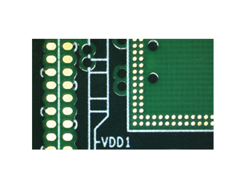
Connecting component terminals through laser penetration and electroplated copper


 Your location: