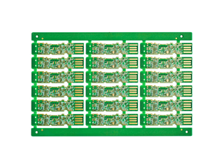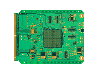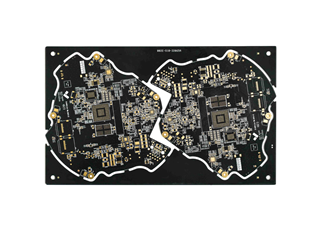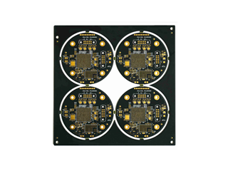
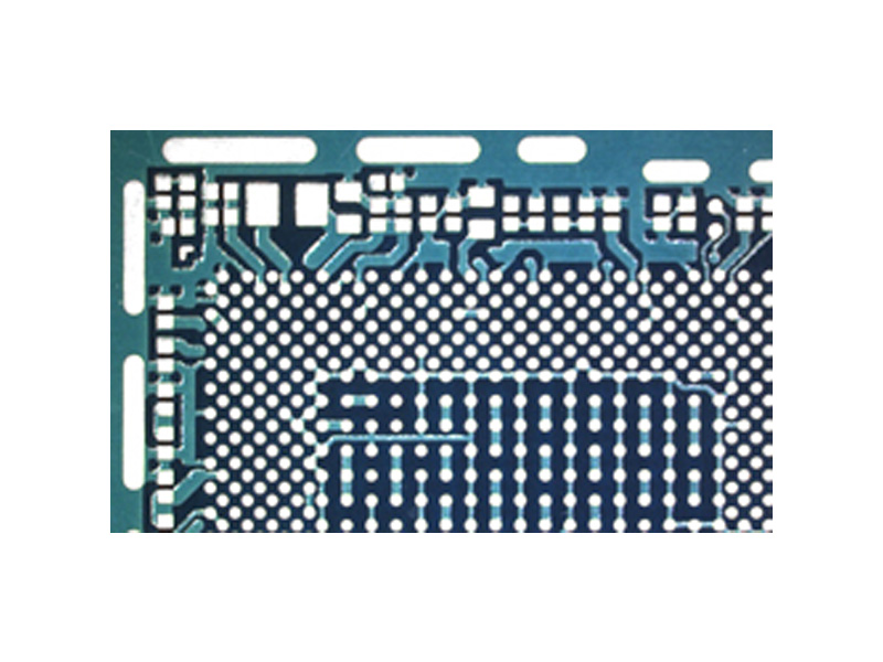


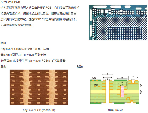
AnyLayer PCB
These are PCBs that can be freely connected between all layers, combining laser technology and fill plating technology to enable ultrafine machining. With higher design freedom and higher density of wiring, these PCBs are perfect for the needs of streamlining and simplifying smartphones and other high-performance devices.
Feature
Anylayer PCB laser is plated by filling in each layer
Thin 0.4mm spacing CSP anylayer interconnection support
Mobile devices for mass production of 10 layer m-via (anylayer PCBs)

 Your location: