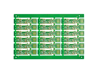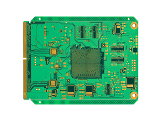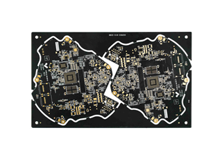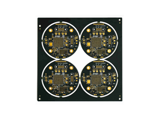


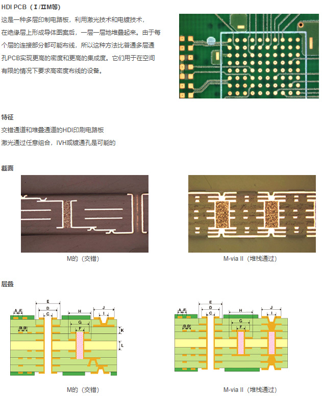
HDI PCB (I/Li IM, etc.)
This is a multi-layer printed circuit board that uses laser technology and electroplating technology to form conductor patterns on the insulation layer and stack them layer by layer. Due to the possibility of wiring at the connection points of each layer, this method achieves higher density and integration than ordinary multi-layer through-hole PCBs. They are used for devices that require high-density wiring in limited space.
Feature
HDI printed circuit board with interleaved and stacked channels
Laser can be used in any combination, such as IVH or plated through holes

 Your location: